![]()
![]()
![]()
![]()
![]()
![]()


|
|
|
|
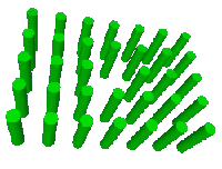
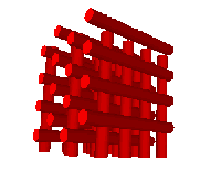
Explaining Photonic Band Gap Materials I have tried to write down some of my interpretations of the Photonic Band Gap field. These are entirely my own views and certainly should not be treated as the definitive statement on the subject !! I hope that you find them useful, any comments, good or bad then please email me !!!!! (areynolds@elec.gla.ac.uk) How best to describe a photonic crystal ? It's an interesting question that rapidly explodes into an exciting and expanding field. The interest in Photonic Crystals covers many applications from sub mm wave microwave reflectors to optical work using synthetically fabricated Opal. In the interests of trying explain the crystals simply I'm going to skip all the analogous behavior with quantum mechanics and electronic band structure calculations that can be found in the solid state field, and try and explain it in conceptually. This is as good an exercise for me in explanation as I hope you find in comprehension !!!! Photonic Crystals are periodic structures, there are natural examples already existing in nature which reflect electromagnetic radiation as propagation through them is prohibited. Present photonic crystal work copies the behavior that is found in nature and scales it to serve the application required. One of the most beautiful and elegant examples of a naturally occurring crystal is the gemstone Opal. The distinctive colour of Opal is due to the reflection of light, the reflection being caused by the photonic band gap of the crystal. If you want to have a look at some already existing computer generated pictures of some commonly used photonic crystals then have a look in the gallery pages. The action of electromagnetic repulsion / reflection, whatever the frequency at which it occurs, is due to the fabric of the crystal. The periodicity of the crystal plays a very important role in the formation of a useful band gap. The actual width of this band gap, expressed either in Hz or in eV which ever unit set is more preferable, depends on the geometry, feature size, spacing and the materials which make up the crystal. A photonic band gap covers a range of frequencies where any incident wave arriving onto the crystal will be reflected rather than transmitted. The simplest analogy is that of a mirror, a mirror reflects light that arrives on it, allowing you to make sure that all is in order before going off to work in the morning !! While a mirror demonstrates the concept of reflection perfectly the behaviour inside a photonic crystal is somewhat more complicated !!! Imagine that we could make the mirror reflect only a particular colour of light............ We have already introduced the concept of periodicity within a structure, and since structures have dimensionality, therefore so do photonic crystals. Photonic crystals can be either 1,2 or 3 dimensional in operation, although all of them in reality are 3 dimensional structures. So what do we mean by dimensionality of a gap ? Photonic Band Gap crystals are generally taylor-made for present applications. They are designed and fabricated to work at a certain frequency, the central, or mid band frequency. The range of frequencies around the central frequency over which the crystal will continue to operate defines the operational bandwidth of the crystal. At present the best band widths that have been achieved represent 20-30% of the centre frequency. Once outside this operation range the photonic band gap nature is no longer seen for that particular crystal !!! Consider a simple square lattice of dielectric cylinders, the lattice geometry is quite separate from the cylinders that are placed at each of the lattice points, it is important to make this distinction. We could also have a cubic lattice but with cylinders consisting of air in a medium of dielectric material. Both lattices will display a photonic band gap but neither centred at the same frequency nor as wide as each other. Another frequently quoted parameter is the fill ratio. The fill ratio defines
the ratio of the feature to the lattice cell in terms of area or volume for
three dimensional crystals. Sometime a feature ratio of radius, or feature
'width' to the lattice spacing is used although this can always be turned into a
fill ratio.
Therefore we can choose to work with either feature ratios or fill ratios depending on which is more appropriate. Lattices can range from square, cubic, hexagonal, tetragonal etc. etc. and the features within them could by cylinders, squares, rectangles, hexagons........ For those people that are familiar with the Bragg interference condition then a photonic crystal uses the very same. Consider a plane wave incident on a periodic structure such as the first row of cylinders in a two dimensional photonic crystal. As a normal wave is incident on the structure it may diffract and scatters but it will also split into forward and reverse waves. As the forward wave continues into the crystal is encounters more and more obstacles that cause more diffraction, scattering and forward and reverse waves. The periodic spacing of the cylinders may lead to the forward and reverse waves inside the crystal to destructively interfere with each other. This generates the photonic band gap ensuring that the radiation cannot propagate through the crystal. Unable to go through the crystal the radiation is reflected. However we note that we have only defined that this condition holds for a particular plane wave incidence angle. For a full band gap to exist every direction should lead to reflection regardless of polarisation. A fully three dimensional band gap will reflect all incident radiation upon it no matter from which direction it comes from for a given frequency, i.e. there are no allowed modes. The Ideal Photonic Band
Gap Crystal....... We need to find a structure that ideally has an infinite number of axis of symmetry within the FBZ in reciprocal lattice space, an impossibility. The structures that we do use have as many axis of symmetry as possible but they still bolt together to form a bulk structure. By adjusting the materials and lattice parameters that are currently available we can design crystals to provide the performance that we require. There are many different methods for modeling the behavior of photonic crystals. All the calculations within these pages have been done using a modified version of the Transfer Matrix Method, the 'TMM' method. The original program code, PHOTON, was written in Imperial College London. The code has since been modified to compute the properties of more complex 2 and 3 dimensional structures and has been integrated with a powerful windows interface to simplify operation. The code can be downloaded from the software page. Within the Photonic Band Gap group in Glasgow we are continually advancing the development, fabrication and modeling of photonic band gap structures. As part of the Opto Electronics Group within the Department of Electronics we host world class research and fabrication facilities, ranging from clean rooms to the latest computer modeling technology. To learn more about the activities and opportunities within the group please visit http://www.elec.gla.ac.uk/groups/pbg/
|
|