![]()
![]()
![]()
![]()
![]()
![]()
![]()

|
|
|
|
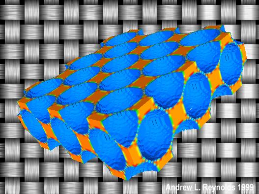
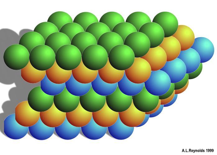
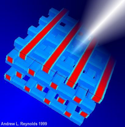
Three dimensional photonic crystals provide three dimensional gaps, that is to say, any wave from any direction will be completely reflected !! One of the many challenges comes from fabricating the structures, especially for optical applications. At present the group is involved in the research of synthetic Opal photonic crystals, representations of which can be seen above. For the millimetre wave regime we are interested in antenna applications of the crystals. The combination of three dimensional photonic crystals and integrated planar antenna technology provides a new exciting approach to a range of advanced efficiency enhanced antenna systems for the future. They may provide a novel reflector technology that can be easily scaled in size to fit almost all intended applications. Within the department we have fabricated and measured PBG woodpile systems with the intention of integrating antennas onto the surface of the structure.( E.Ozbay in Optical Letter, Aug. 1994. The paper 'Tera-Hertz spectroscopy of three dimensional photonic band gap crystals' outlines a recipe for a structure that exhibits a fully three dimensional band gap centred at 500 GHz.) The technological advances in material processing in the semiconductor industry are now being utilized in the field of antennas. Techniques such as micro machining and etching now allow antennas and their associated components to be readily reproduced and integrated onto a single chip. The drastic size reduction and excellent reproducibility has opened up a whole new rapidly developing field of advanced integrated antenna systems. Integrated antenna systems may find applications ranging from environmental monitoring of the ozone hole to all weather visual systems for aircraft. The ability to place a complete integrated antenna system on top of one small section of a semiconductor wafer is now a reality. The semiconductor substrate is processed so that it acts as a reflector, such a substrate is then called a photonic band gap crystal. The crystal forbids the propagation of electromagnetic radiation through itself, reflecting any radiation such as that from an antenna system that is placed upon it. The key to their operation is through their periodicity, the pattern and the repetitive spacing that makes the periodicity of the crystal also plays a vital role in its character, different patterns induce different properties. Systematic etching, stacking and rotating of semiconductor wafers makes the "woodpile" system. A periodic bar pattern is etched from each wafer. The wafers are then stacked vertically, each consecutive layer rotated with respect to the previous one. This builds a system that repeats every four wafers, forming a photonic band gap crystal. An antenna can then be placed on top of the stack that then must radiate into free space, ideally with no power loss into the crystal. Photonic Crystals present a tremendous opportunity for the future, they reduce the mass of a system, increase the efficiency and are simple to manufacture, all features that are essential antenna systems.
|
|