![]()
![]()
![]()
![]()
![]()
![]()
![]()


|
|
|
|
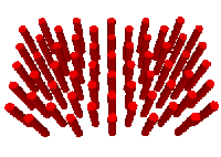
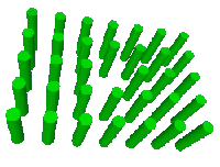
At present there is a substantial interest in 2 dimensional photonic band gap
structures. There are of course more than one type of 2 dimensional lattice, we
have already met the square lattice of cylinders, but there are others such as
the hexagonal lattice, honey comb lattice and many more.
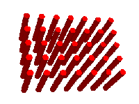
There are many options to the lattice also, we do not necessarily have to
pick cylinders all the time, we could use bars, rectangles, triangles or even
hexagonal features placed in the lattice. It is also important to note that
often we fabricate the inverse of these structures, that is to say cylindrical
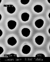
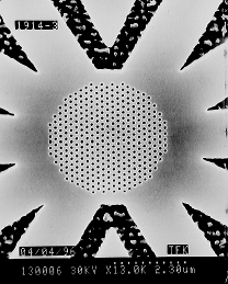
air features in an embedding medium of dielectric material as is shown below. In
this structure Thomas Krauss
has fabricated a 2 dimensional array of air cylinders into a dielectric medium,
it is a close up view of the centre of the structure shown to the right in the
table. If you want a closer look at either of the structures just click on them
!!!
So what about the 2 dimensional gap ? What does this mean ? It means that if we have a wave incident onto our structure from any direction within the same 2 dimensional plane as the periodicity of the crystal then it will always be reflected !!! This of course is limited to a range of frequencies, but we can achieve quite reasonable band widths (band width = gap width / central gap frequency). Repetitive rows of periodically spaced cylinders ensure that the two dimensional periodicity holds in only one plane. Therefore if we restrict the incident radiation to this plane then for the correct filling ratios and material constants and polarization of the wave then we expect to observe a complete two dimensional band gap. This is indeed the case !!! It does not matter from which angle we bombard the structure from so long as we are within the two dimensional plane. If we move out of the plane then the special periodicity that we have deliberately set up becomes increasingly compromised the more we stray from it. Consequently we see a marked decrease in photonic band gap behaviour. Right lets take a hop back and have a look at the response from a 2 dimensional crystal of dielectric rods. I have looked at a fairly standard system, something very similar to that presented by Pierre R. Villeneuve, Shanhui Fan, and J.D. Joannopoulos, in their paper Microcavities in Photonic Crystals, Mode symmetry, tunability, and coupling efficiency. Physical Review B, Volume 54, Number 11. Here I present both the perfect crystal, defect crystal and the transmission
response for them both. It is also worth mentioning here that the above are
results I have computed, therefore do not assume that they are absolutely
correct !!
Analysis : What can we see from the above ? There are a few points to note concerning the above analysis, firstly that it has been carried out for one direction only, and does not represent the complete two dimensional gap. In order to facilitate the understanding of what I mean by 'only one direction' I'm going to have to introduce Brillouin Zones, not in any great detail but just to aid understading of the above. Without explaining too much the analysis above was carried out in the Gamma X direction, I'll try and write a section on Brillouin Zones and post it here on the web soon. If you would like me to tell you about this when it happens please join the PBG mailing list, this will shortly be integrated (I hope) with the groups activities and will bring you news about all of our activities and not just me !!!!
|
|
 Two Dimensional
Lattice
Two Dimensional
Lattice