![]()
![]()
![]()
![]()
![]()
![]()
![]()


|
|
|
|
To find out more about the structures follow the links below, there are examples, analysis and results !!!
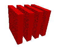
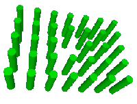
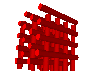
One Dimensional In the above table showing the crystals we can
see examples displaying the 1,2 or 3 dimensional periodicity of some elementary
crystals. For the moment we can ignore the cylinder that is missing from our 2
dimensional structure, this introduces a defect into the crystal but we'll talk
more about that later. For the moment let's take a look at the response of
the 1 dimensional structure, (something similar to a Bragg stack). We bring a
wave onto the structure that is normal i.e. perpendicular to the first flat
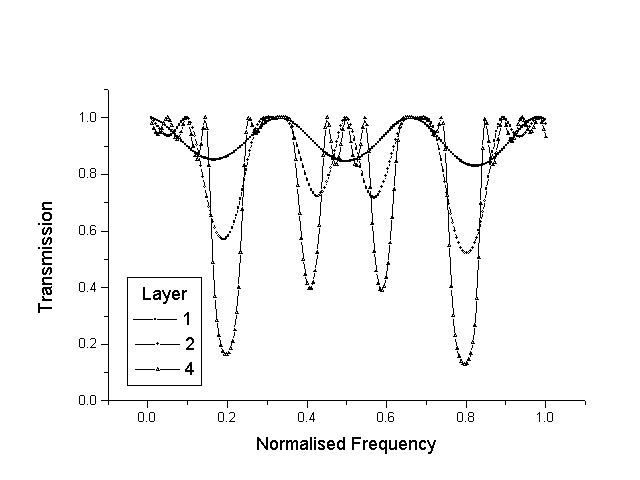
face. We find a response something like the following (if you want a closer look
at the response click on the image !)
In the figure we have plotted the transmission through the structure against normalised frequency for a few layers, or periods of the crystal. There are several things to learn here, we can see that as the crystal becomes thicker (has more periods) then the transmission response for some frequencies rapidly goes towards zero. However at the same time, the width of these troughs decreases, so if we are looking for a wide band of frequencies that do not transmit we have a trade off, nothing in life is ever simple !!! One dimensional systems such as the one described and depicted in the figure above are actually used, they can be taylor made to provide either reflection or anti reflection coatings. This is done by careful consideration of the materials used, their thickness and the number of layers, ever wondered how those mirror sunglasses worked.......??????!!!!!!!! Before moving on to two dimensional crystals lets back up a little and
introduce some other one dimensional structures. One of the other tools
frequently used with the PBG subject area is that of the band structure diagram,
and no better place to introduce the concept than in one dimension. One of the
most important relations in electromagnetics, especially PBG, (and not
forgetting Maxwell' Equations !!) is the dispersion relation:
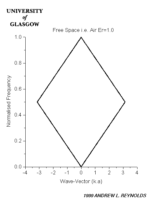
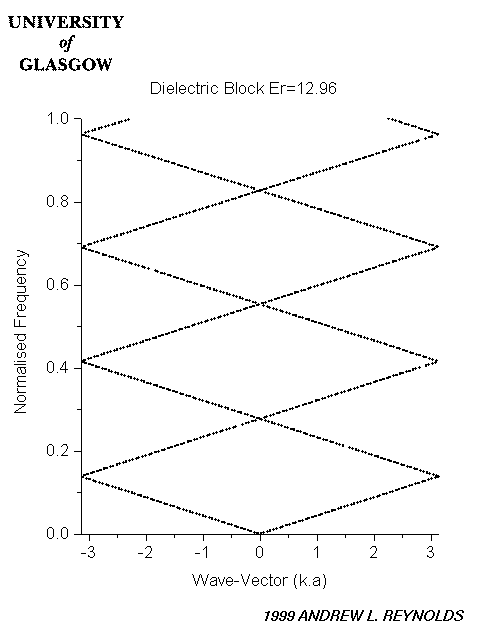
(w=omega, n=refractive index, c=speed of light in vacuo, k=wave vector). Such a simple relation, but what does it mean ? To start with consider a 'piece' or 'block' of air, strange concept I know but when we take lots of blocks all together then we just have 'free space', simple enough ? Right we have a piece of air, what modes can be supported within it, we have
no waveguide to worry about, no bits of metal, no PBG crystal for the moment, in
fact the answer is all of them !!!! So what does this look like, and while we
are at it, for the sake of comparison and for comprehension what happens if we
have a block of dielectric material and not air, what modes do we have then ?
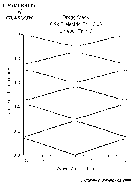
From the two diagrams we can see that we have a diamond shape that repeats, why ? Before we answer that question let's think about why the number of diamonds is different between the air and dielectric. Going back to the free space dispersion relation wn=ck then clearly if we change n, which remember is the refractive index, not dielectric constant, then we should clearly alter the gradient of the line. This we have done, you should be able to see that straight away, but why do the lines double back on themselves when they reach the sides of the plots ? Well the answer to this lies with the fact that we have chosen a 'piece' of air, with an artificial periodicity so our expected straight line of constant gradient gets folded up. When we reach the sides of the plots the band doesn't just disappear, so it continues with the same gradient by folding. That hopefully explains where the diamond shape comes from !!! We have already touched a little on Bragg Stacks, but armed with our new knowledge over bands let's take another look, and make a comparison with some published material. If we go back to our band diagram for our solid block of dielectric material we clearly saw the repeating diamond shape. A Bragg stack is a mixture of two materials, and if we get the ratios right (ratio of the thickness of one material to the other) then we can open up some useful gaps in the band diagram and we find so called 'Photonic Band Gaps' !!!! Remember that a gap in the band diagram means that a wave cannot propagate, no band means no propagation, hence no transmission.......let's check !!!! Rather than jumping straight into out first 'proper' Bragg stack, we'll start
by introducing a thin layer of air into our block of dielectric material. Below
we can see that in the centre of the plot and the edges for the system with a
little air that we have a small region where there are no bands ! To give you
the specifics, our block of dielectric is 0.9a and the air 0.1a,
where a is the periodicity or lattice constant of the grating ! As per
usual, if you want a closer look at the plots just click !!!
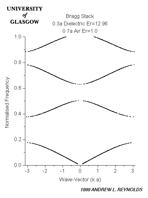
If we increase the ratio of air to dielectric, in fact quite considerably so
that in the end we have 0.7a air and 0.3a dielectric then we can
open some useful gaps. I have picked these values so that you can make a
comparison with the paper from Andrew Ward, Calculating
Photonic Green's Functions Using a Non-Orthogonal Finite Difference Time Domain
Method. A.J. Ward and J.B. Pendry, Physical Review B, 58, 7252, (1998). NOTE
however that these calculations were done with the transfer matrix method, as
was also suggested by Imperial College (Transfer Matrix Techniques for
Electromagnetic Waves. J.B. Pendry and P.M. Bell, in "Photonic Band Gap
Materials", NATO ASI Series E: Applied Sciences - Vol. 315, edited by C.
M.Soukoulis (Kluwer, Dordrecht, 1996), p. 203. )
Summary 1D We have shown with both band diagrams and transmission plots that if we choose our materials, their associated dielectric constants and thickness' correctly that we can open useful photonic band gaps. We have also discussed The Dispersion Relation and hopefully explained why we have the repeating diamond shape within the band structure. One dimensional photonic band gap structures 'Bragg Stacks' are used within laser cavities and for optical coatings. Generally a one dimensional gap is only of use if our application is going to be restrained to a specific, or small range of angles if we have a source embedded within the dielectric medium.
|
|